Keynote Speakers

speaker

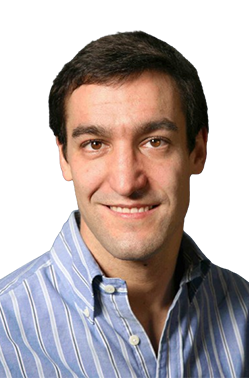
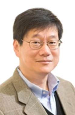
Jamal Deen

Professor at McMaster University

Bio.: Distinguished University Professor; Senior Canada Research Chair in Information Technology; Director, Micro- and Nano-Systems Laboratory (MNSL); President, Academy of Science, Royal Society of Canada (2015-17); FRSC Fellow, Royal Society of Canada; A-CAS Academician (Foreign Member), Chinese Academy of Sciences; FCAE Fellow, Canadian Academy Engineering; FNASI Fellow (Foreign), National Academy of Sciences, India; FINAE Fellow (Foreign), Indian National Academy Engineering; MEASA Member, European Academy of Sciences and Arts; FTWAS Fellow, The World Academy of Sciences; FIEEE Fellow, Institute of Electrical & Electronics Engineers; FAPS Fellow, American Physical Society; FECS Fellow, Electrochemical Society; FAAAS Fellow, American Association for the Advancement of Science; FEIC Fellow, Engineering Institute of Canada.

In the couple of few decades, the field of flexible organic/polymeric electronics has advanced significantly. This has been primarily because of the developments of new materials, improvements in the quality organic/polymeric materials, as well as the processing techniques, technologies and device designs. For example, roll-to-roll, sheet-to-sheet or printing technologies are being proposed as suitable manufacturing candidates because they can be carried out at room temperature, do not require the kind of clean room environment needed for traditional semiconductor manufacturing, and are very suitable for very low-cost, high volume production. Further, these advances are mostly stimulated by the promise of lighter and more robust devices and systems for applications that include large-area electronics, active matrix large-area displays, large-area solar cells, interactive displays, and conformable sensors and actuators. However, despite these advances, there remain challenges in the large-scale transfer of research prototypes into manufactured products. Furthermore, a major the limitation is the lack of accurate and computationally efficient compact models for organic/polymeric thin film transistors with associated parameter extraction techniques. In this presentation, we will discuss recent compact models and illustrate the merits and limitations of several of them as part of the electronic design automation platform. In this presentation, we will discuss our progress in developing industry-viable static and dynamic compact models for flexible transistors with predictable performance and the associated parameter extraction schemes including evolutionary computation for parameter extraction. Finally, we will present several on-going modeling challenges including illumination, hysteresis and contacts effects, as well as models that can predict stability, reliability, and lifetime.
speaker

David Atienza Alonso

Professor at Embedded Systems Laboratory, EPFL

Bio.: David Atienza Alonso is a professor of Electrical and Computer Engineering, Head of the Embedded Systems Laboratory (ESL) and Scientific Director of the EcoCloud Sustainable Computing Center at EPFL, Switzerland. He received his MSc and Ph.D. degrees in computer science and engineering from UCM, Spain, and IMEC, Belgium, in 2001 and 2005, respectively. His research interests include system-level design methodologies for high-performance multi-processor system-on-chip (MPSoC) and low-power Internet-of-Things (IoT) systems, including new 2-D/3-D thermal-aware design for MPSoCs and many-core servers, ultra-low power edge AI architectures for wireless body sensor nodes and smart embedded systems, HW/SW reconfigurable systems, dynamic memory optimizations, and network-on-chip design. He is a co-author of more than 400 papers, two books, and has 14 licensed patents in these topics. He served as DATE General Chair and Program Chair, and is currently Editor-in-Chief of IEEE TCAD. Among others, Dr. Atienza has received the ICCAD 2020 10-Year Retrospective Most Influential Paper Award, the 2018 DAC Under-40 Innovators Award, and an ERC Consolidator Grant. He is a Fellow of IEEE, a Fellow of ACM, served as IEEE CEDA President (period 2018-2019) and in the IEEE CASS BoG, and is currently the Chair of the European Design Automation Association (EDAA).

The soaring demand for computing power in this AI era has produced as collateral undesirable effects a surge in power consumption and heat density for computing systems. With the rising cooling costs and challenges in heat removal in the latest nano-scale and heavily heterogeneous multi-processor system-on-chip (MPSoC) designs targeting the execution of the latest generative AI algorithms, the development of accurate but fast thermal modeling frameworks to develop dynamic thermal management (DTM) approaches have become indispensable.
These new approaches strongly depend on the availability of efficient and scalable methodologies for thermal and power modeling, analysis, and characterization of computing systems at multiple abstraction levels. These methodologies must provide the appropriate accuracy to capture the thermal diffusion mechanisms in 2D and 3D AI chips and fast adaptation for the design space exploration of MPSoCs architectures and the latest cooling technologies. In this talk, Prof. Atienza will review the basis of the recent innovative thermal modeling and prototyping approaches for non-uniform thermal characterization included in the open-source 3D Interlayer Cooling Emulator (3D-ICE). Then, in conjunction with a fast offline application profiling strategy utilizing gem5-X, the latest open-source architecture simulator for 2D/3D MPSoCs designs targeting AI chips, it will be shown how it is possible to develop a complete DTM evaluation framework that can be used to create Multi-Agent Reinforcement Learning (MARL) control schemes for different 3D MPSoCs and AI accelerators. Finally, it will be illustrated how this DTM framework based on MARL control can support advanced liquid cooling and electricity-generation technologies using microfluidic power cells for the next generation of energy-efficient 2D and 3D AI accelerators.

speaker

Xiaoqing Wen

Professor at Kyushu Institute of Technology

Bio.: Xiaoqing WEN received the B.E. degree from Tsinghua University, China, in 1986, the M.E. degree from Hiroshima University, Japan, in 1990, and the Ph.D. degree from Osaka University, Japan, in 1993. He was an Assistant Professor at Akita University, Japan, from1993 to 1997, and a Visiting Researcher at the University of Wisconsin–Madison, USA, from Oct. 1995 to Mar. 1996. He joined SynTest Technologies Inc., USA, in 1998, and served as its Vice President and Chief Technology Officer until 2003. He joined Kyushu Institute of Technology, Japan, in 2003, where he is currently a Professor with the Department of Computer Science and Networks. He is a Co-Founder and Co-Chair of Technical Activity Committee on Power-Aware Testing under Test Technology Technical Council (TTTC) of IEEE Computer Society. He is serving as Associate Editors for IEEE Transactions on Very Large Scale Integration Systems (TVLSI) and Journal of Electronic Testing: Theory and Applications (JETTA). He co-authored and co-edited the latest VLSI test textbook in 2006 and the first comprehansive book on power-aware VLSI testing in 2009. His research interests include design, test, and diagnosis of LSI circuits. He has published more than 300 papers and holds 43 U.S. patents & 14 Japan patents. He received the 2008 Society Best Paper Award from IEICE-ISS. He is a Fellow of IEEE.

With low power consumption becoming a key requirement for advanced LSI designs, the gap between functional power and test power has kept growing to such an extent that power-aware testing has now become a must. The foundation of power-aware testing is a complete understanding of the global impact of switching activity on peak and average power as well as the local impact of switching activity on IR-drop-induced delay increase along data and clock paths. This talk presents a holistic view on various aspects of power-aware testing, aimed at helping researchers and engineers to develop more sophisticated and complete solutions for controlling LSI test power.

speaker

John Kim

Professor at KAIST (Korea Advanced Institute of Science and Technology)

Bio.: John Kim is currently a full professor in the Schoolof Electrical Engineering at KAIST (Korea Advanced Institute of Science and Technology) in Daejeon, Korea. John Kim received his Ph.D. from Stanford University and B.S/M.Eng from Cornell University. His research interests include computer architecture, interconnection networks, security, and mobilesystems. He has received a Google Faculty Research Award,Microsoft-Asia New Faculty Fellowship,and is listed in the Hall of Fame for ISCA, MICRO,and HPCA. He has also worked on the design of several microprocessors at Intel and at Motorola.

As compute and memory continue to scale, the interconnect or the communication is becoming a critical bottleneck in determining overall system performance and scalability. In this talk, I will present the challenges of the "hidden" interconnect that exists in modern systems in terms of its impact on the design, performance, reliability/security, and cost of the system. In particular, I will present case studies from recent interconnect architectures.

speaker

Sreejit Chakravarty

Distinguished Engineer at Ampere Computing

Bio.: Dr. Sreejit Chakravarty is an IEEE Fellow, a highly recognized Researcher, Inventor, and a Distinguished Engineering Leader, with extensive industry and academic experience. He is currently a Distinguished Engineer at Ampere Computing, Santa Clara, CA, USA where he drives the strategic initiatives for product quality. Prior to this, he had over 25 years of industry experience as a Principal Engineer with Intel Corporation and Distinguished Engineer at LSI and AVAGO. He started his career in academia as an Associate professor of Computer Science, at The State University of New York at Buffalo, where his work was funded by multiple National Science Foundation Grants. He has architected innovative solutions across the entire silicon life cycle spanning Silicon Quality and Reliability (RAS, Functional Safety and Silent Data Errors) and subsequently drove them from concept to product intercept. He has published 1 book, authored 145+ IEEE papers, has 23 issued US patents, graduated several doctoral students, served in various capacities at numerous IEEE conferences, and delivered multiple keynote addresses. He has mentored research at several universities like Princeton, USC, UIUC, etc. For his professional work, he has been recognized as an IEEE Fellow and SUNY Distinguished Alumni. He currently chairs the IEEE Study Group on Chiplet Interconnect Test and Repair, which aims to standardize the test and repair of chiplet interconnects which will lay the foundation to realize the chiplet revolution.

Chip-let based design is here to stay and, fueled by various advanced packaging technologies, it is projected to revolutionize the semiconductor industry. This talk will discuss the following:
(i) the interconnect test and repair problem;
(ii) the need for and the ongoing effort, under IEEE P3405, to standardize interconnect test and repair; and
(iii) EDA challenges in accomplishing a standardized interconnect test and repair solution.

speaker

Christopher Thomas

Visiting Professor, Tsinghua University & Former Managing Partner, Asia Semiconductor Practice, McKinsey & Company

Bio.: Chris Thomas was most recently a partner with McKinsey & Company. He served as co-Managing Partner for the Firm’s Global Digital Strategy service line as well as its Global IoT service line; and as the leader of its Asia Semiconductor Practice. Prior to McKinsey, Chris spent ten years at Intel. He was the General Manager of Intel China, with joint ownership for the region’s $5 billion-plus P&L. In this role, he grew revenues by more than 50% and oversaw China’s successful elevation from a sales unit to an independent regional P&L business reporting directly into headquarters. He also led several business units in the Silicon Valley headquarters. Chris began his career as a private equity investor at The Blackstone Group in New York City. Chris is a Visiting Professor at Tsinghua University, China’s leading educational institution. He received an MBA from Stanford Business School, where he was an Arjay Miller scholar; a Master of Arts in Political Science from Stanford University; and a Bachelor of Science in Economics, summa cum laude, from the Wharton School.

speaker

Elyse Rosenbaum

Professor at University of Illinois

Bio.: Elyse Rosenbaum is the Melvin and Anne Louise Hassebrock Professor in Electrical and Computer Engineering at the University of Illinois Urbana-Champaign. She received a Ph.D. in electrical engineering from University of California, Berkeley. She is the director of the Center for Advanced Electronics through Machine Learning (CAEML), a joint project of the University of Illinois, North Carolina State University, and Penn State University. Her current research interests include CDM-ESD reliability, ESD-robust high-speed I/O circuit design, compact modeling, optimization of heterogeneously integrated system-in-package, and machine learning aided modeling of circuit lifetime distributions. Dr. Rosenbaum has authored or co-authored over 200 technical papers; she has been an editor for IEEE Transactions on Device and Materials Reliability and IEEE Transactions on Electron Devices. She served as the General Chair of the 2018 International Reliability Physics Symposium. Dr. Rosenbaum was the recipient of a Best Student Paper Award from the IEDM, an Outstanding Paper Award and 2 Best Paper Awards from the EOS/ESD Symposium, a Technical Excellence Award from the SRC, an NSF CAREER award, an IBM Faculty Award, and the ESD Association’s Industry Pioneer Recognition Award. She is a Fellow of the IEEE.

ESD protection circuits degrade circuit performance and/or consume valuable Si area. Thus, a conservative approach to ESD device sizing is undesirable. To avoid ESD overdesign without compromising the ability to meet ESD specifications on the first silicon spin requires that ESD designs be validated by circuit simulation. In this talk, I will describe some of the compact models used for ESD simulations and present various case studies.

speaker

Jacky Ni

Founder /CEO of Advanced Manufacturing EDA Co., Ltd

Bio.: Jacky Ni, founder and CEO of Advanced Manufacturing EDA Co., Ltd. (AMEDAC). Mr. Ni dedicated in EDA development for more than 20 years with a wealth of experience and contribution in the China EDA industry, and used to be experienced in EDA product innovation, market development, corporate strategy and management, etc.. Prior to AMEDAC, Mr. Ni served as Deputy General Manager of Synopsys China, a global leading EDA company. During his more than 13-year tenure at Synopsys, Mr. Ni was used responsibility for corporate strategy and implementation, product planning and development, R&D management, sales operations and product application. Mr. Ni successfully boosted the market share of Synopsys in the field of Foundry Business in China, and used to serve multiple leading companies across the IC value chain and end application firms. Since Mr. Ni started to lead Synopsys China Foundry Business, he and his team were honored with excellent supplier award of important clients including SMIC’s 28nm Outstanding Contribution Award, that proved the industry’s recognition of Mr. Ni’s contribution. After Synopsys, as COO of Alchip (a famous chip design service company), Mr. Ni successfully repositioned the company as the leader in AI chip design service, by refining the strategy and vision of Alchip, transforming the corporate organization to improve efficiency and lead business innovation. Mr. Ni founded AMEDAC in 2019. Utilizing his management practice and extensive network in the EDA field, Mr. Ni has led AMEDAC to be the first supplier to provide self-developed manufacturing EDA software, which solves the most important technical shortcomings of domestic EDA. Mr. Ni along with this 5-year-old company, has covered full flow EDA tools for advanced chip manufacturing, and moves a big step towards intelligence integration of EDA.

Generative AI represented by LLM has demonstrated excellent and versatile solution capabilities. It has proven useful in a range of applications and the EDA field has begun to rapidly adopt the LLM model recently. The evolution of EDA has been accerlated by generative AI technologies, and the cutting-edge technolohgy has shown its contribution to many field, including large-scale data process, engineering effciency improvement, work flow integration, etc., which reveals Generative AI‘s transformative power on chip design and implementation. As chip shrinking, structures becoming more complex, and 3D-IC developing, manufacturing EDA plays more important role in the value chain. The implementation of manufacturing EDA is based on entensive professional data and experience, various mathematical and physical algorithms, which is consistent with the core value of LLM. Thus, we have seen many application of generative AI in the field of manufacturing EDA, including ViT in patterning, LLM in smart manufacturing and LLM using for manufacturing flow integration. Further, some of the most cutting-edge developments demonstrate the potential of generative AI to integrate the entire process from design to manufacturing to 3D advanced packaging, that could change the EDA development model. We have moving a step on explore generative AI in manufacturing EDA. Based on the data, knowledge accumulation and our understanding on artificial intelligence embedding in EDA software, we have already achieved good results in fields such as AI copilot in chip manufactruing, AI generating code and AI integrating chip implemention flow. By leveraging generative AI technology, It can realize automatic integrated processes and interconnections from design, process, manufacturing to 3D packaging, thereby greatly improving the efficiency of advanced chip R&D and production.

speaker

Sa Zhao

Vice President of Engineering in Semitronix Corporation

Bio.: Ms. Sa Zhao received her B.S. in Physics from Peking University and M.S. in Physics from Purdue University. With over 25 years of semiconductor industry experience, Ms. Zhao currently serves as Vice President of Engineering in Semitronix Corporation, focusing on Manufacturing EDA and IC Yield Ramp services. Prior to Semitronix, Ms. Zhao worked with world-leading fabs and design houses on yield enhancement, device optimization, DFM technologies, inline control methodologies. Through her visionary leadership and strategic insights, Semitronix pushed the boundaries of conventional yield management & control systems, harnessing the power of AI and ML to unlock new levels of performance and efficiency to enhance product yield, quality, and reliability.

In the prevalent foundry-design house eco-system, achieving optimal yield outcome requires close engagement between players. An integrated data framework is a key enabler for such collaborations, where product and process insights meet. In this talk, we propose a complete work-flow where design-side DFT (design-for-test), diagnostics and product layout features are combined with production data and proprietary fine-grained process monitors to facilitate the efficient identification/quantification of yield drivers and mechanisms. This understanding, in turn, supports both fab-side production improvements and design-side DFM (design-for-manufacturing) mitigations.

speaker

Han Yu

Marketing Cooperation Director of Empyrean Technology

Bio.: Yu Han, with the Chinese National Senior Engineer Title, graduated from Beihang University with Master Degree in 2007. He worked for Empyrean Technology Corp.(Empyrean) from 2010 till now. He is now the Senior Technical Marketing Director of Empyrean, leading some business including external technical corporation and university programs. He has published over 10 articles on academic journals such as IEEE-DAC, ACM-GLSVLSI, China Integrated Circuit etc. as the first author. He has also served as a review expert of the "National Project of Micro-Nano Electronics", the deputy director of the editorial board of "National Vocational and Technical Skill Standards - Integrated Circuit Engineering", and the director of Guangdong EDA Engineering Center.

This presentation will show some commercial EDA tool having used AI Algorithm like machine learning and neural network. It will also discuss the possible applications of big language model in EDA field.

speaker

Mehdi B. Tahoori

Professor at KIT (Karlsruhe Institute of Technology)

Bio.: Mehdi B. Tahoori is Professor and the Chair of Dependable Nano-Computing at Karlsruhe Institute of Technology (KIT), Germany. He received the B.S. degree in computer engineering from Sharif University of Technology, Tehran, Iran, in 2000, and the M.S. and Ph.D. degrees in electrical engineering from Stanford University, Stanford, CA, in 2002 and 2003, respectively. He is currently the deputy editor-in-chief of IEEE Design and Test Magazine. He was the editor-in-chief of Elsevier Microelectronic Reliability journal. He was the program and general chair of IEEE VLSI Test Symposium in (VTS) and General Chair of IEEE European Test Symposium (ETS). Prof. Tahoori was a recipient of the US National Science Foundation Early Faculty Development (CAREER) Award in 2008 and European Research Council (ERC) Advanced Grant in 2022. He has received a number of best paper nominations and awards at various conferences and journals. He is currently the chair of IEEE European Test Technologies Technical Council (eTTTC). He is a fellow of the IEEE.

Printed electronics is an emerging and fast-growing field which can be used in many demanding and emerging application domains such as wearables, smart sensors, and Internet of Things (IoT). Unlike traditional computing and electronics domain which is mostly driven by performance characteristics, printed and flexible electronics based on additive manufacturing processes are mainly associated with low fabrication costs and low energy. Printed electronics offer certain technological advantages over their silicon-based counterparts, such as mechanical flexibility, low process temperatures, maskless and additive manufacturing possibilities. Neverteless, due to low device count, large feature sizes and high variabilities, originated in low-cost additive manufacturing, existing design automation and computing paradigms of digital VLSI are not applicable to printed electronics. This talk covers the technology, process, modeling, fabrication, design automation, and computing paradigms for circuits and systems based on additive printed technologies.